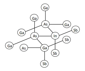
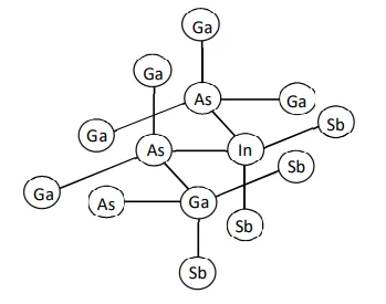
Author: Asatova Umida Palvanovna
Abstract:
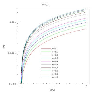
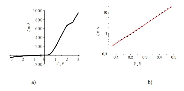
n-GaPp-(InSb)1-x(Sn2)x (0 х 0.05) heterostructures were fabricated and their current-voltage characteristics were studied. At low voltages V < 0.5 V the current-voltage characteristic is described by the exponential law: I = I0exp (qV / ckT) with an exponent c = 3.6, and at large voltage from 0.5 to 1.8 V by power laws: I = AVm with different values of coefficient A and exponent m at various voltages. At higher voltages - from 2.10 to 2.48 V a sublinear section is observed, it is described by the law: V = V0exp(Iad / S). The results are explained by the diffusion-drift mechanism of current transport conditions of dielectric relaxation, as well as the effect of injection depletion.


Author: Saidov Amin Safarbayevich, Usmonov Shukrullo Negmatovich, Asatova Umida Palvanovna, Tolmas Ishniyazov
Abstract:
Layers of solid solutions (InSb)1-x(Sn2)x on (100) GaAs and (100) GaP substrates were grown by liquid phase epitaxy from an indium melt solution. The solid solution (InSb)1-x(Sn2)x (0 х 0.05) had a mono-crystal structure with the orientation (100), constant of the lattice as.s. = 6.486 Å and the hole conductivity type. The spectral dependence of the absorption coefficient was used to estimate the band gap of the epitaxial layer of the solid solution, which was 0.11 eV. The spectral photosensitivity of n-GaAs–p-(InSb)1-x(Sn2)x and n-GaP–p-(InSb)1- x(Sn2)x heterostructures covers the wavelength range from 1.0 to 5.3 μm.


Author: Saidov А. S, Asatova U.P, Ismailov Sh.K., Usmonov Sh.N.
Abstract:
In this article the parameters of pSi1-xGex solid solution was simulated by using TCAD Sentaurus program. The gap dependence on composition of solid solution was carried out. A current-voltage characteristics of the structure was simulated at different composition as well as at different carrier concentration in the film.