 STRUCTURAL FEATURES OF SOLID SOLUTIONS (InSb)1-x(Sn2)x FILMS GROWN FROM A LIQUID PHASE ON GaAs SUBSTRATES AND SOME PHOTOELECTRIC PROPERTIES OF HETEROSTRUCTURES ON THEIR BASIS
Author: Saidov Amin Safarbayevich, Usmonov Shukrullo Negmatovich, Asatova Umida Palvanovna, Tolmas Ishniyazov
Abstract:
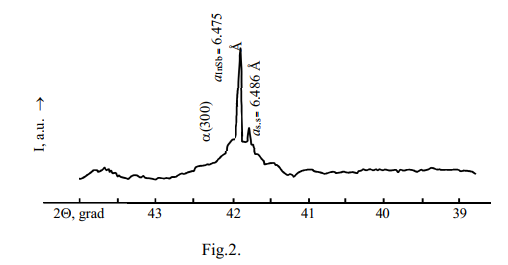
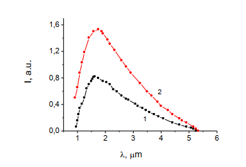
Layers of solid solutions (InSb)1-x(Sn2)x on (100) GaAs and (100) GaP substrates were grown by liquid phase epitaxy from an indium melt solution. The solid solution (InSb)1-x(Sn2)x (0 х 0.05) had a mono-crystal structure with the orientation (100), constant of the lattice as.s. = 6.486 Å and the hole conductivity type. The spectral dependence of the absorption coefficient was used to estimate the band gap of the epitaxial layer of the solid solution, which was 0.11 eV. The spectral photosensitivity of n-GaAs–p-(InSb)1-x(Sn2)x and n-GaP–p-(InSb)1- x(Sn2)x heterostructures covers the wavelength range from 1.0 to 5.3 μm.
 STRUCTURAL FEATURES OF SOLID SOLUTIONS (InSb)1-x(Sn2)x FILMS GROWN FROM A LIQUID PHASE ON GaAs SUBSTRATES AND SOME PHOTOELECTRIC PROPERTIES OF HETEROSTRUCTURES ON THEIR BASIS
Author: Saidov Amin Safarbayevich, Usmonov Shukrullo Negmatovich, Asatova Umida Palvanovna, Tolmas Ishniyazov
Abstract:
Layers of solid solutions (InSb)1-x(Sn2)x on (100) GaAs and (100) GaP substrates were grown by liquid phase epitaxy from an indium melt
solution. The solid solution (InSb)1-x(Sn2)x (0 ≤х≤ 0.05) had a mono-crystal structure with the orientation (100), constant of the lattice as.s. = 6.486 Å and the hole conductivity type. The spectral dependence of the absorption coefficient was used to estimate the band gap of the epitaxial layer of the solid solution, which was 0.11 eV. The spectral photosensitivity of n-GaAs–p-(InSb)1-x(Sn2)x and n-GaP–p-(InSb)1-x(Sn2)x heterostructures covers the wavelength range from 1.0 to 5.3 μm.